
Choosing the best PCB for your project involves several considerations. There are various types of PCBs available, including surface mount, multilayer and double-layer PCBs. Before you buy, you should know how to choose the type of PCB that will provide you with the most accurate results.
Single-layer
Choosing the right single-layer PCB is important for any PCB project. There are several factors to consider, including cost, base material, and size. These will help you determine the best choice for your project.
Single-layer PCBs are commonly used in many types of electronic devices. These include small household appliances, power supplies, and even LED lights. They are also widely used in the design of radios and calculators.
The basic function of a PCB is to transfer signals and electrons between layers. These are then connected through tiny holes in the board. The PCB’s thickness depends on the circuit’s purpose.
The conductive layer transmits signals and the base layer holds the electrical components in place. The dielectric layer is also an important part of a PCB. Most PCBs use a dielectric material called FR-4, which is made of fiberglass and epoxy. This dielectric is inexpensive and provides good heat resistance.
Using a single-layer PCB will save you time and money. It is also easier to produce than multi-layer PCBs. However, you may want to consult an experienced designer to make sure you’re making the best choice for your project.
Double-layer
Printed circuit boards are available in two basic types: single and double layer. The latter type is preferred by most electronic device makers.
Unlike a single sided board, a double sided PCB has a conductive layer on both sides. This enables components to be mounted on the same side of the board. The circuits are inserted through tiny holes called through-holes.
Using a double sided PCB is beneficial for complicated electronics. It allows for more components in a small space, without the need for point-to-point soldering. It also provides more durability.
A double sided board consists of a substrate layer and a conductive layer. In the middle is an insulating layer. These are sandwiched together by a dielectric layer, which is then covered with a soldermask.
The manufacturing process for a two-layer PCB is simpler than for a single-sided PCB. The first step is to lay down the substrate and conductive layers. Then, the dielectric layer is laminated with copper on both sides. This is done by a photolithography process.
Multilayer
Unlike a single sided PCB, a multilayer PCB consists of three or more conductive layers stacked on top of each other. Each layer is separated by a dielectric material. The thickness of the copper layer varies depending on the type of board.
The most important feature of a multilayer PCB is its signal integrity. For the best performance, traces must be able to handle the load of a signal with controlled impedance. The design of a multilayer PCB must also be considered. Choosing the wrong layer can cause circuit malfunctions and overshoot.
A well designed copper trace can carry current without causing electrical resistance. On the other hand, a poorly designed trace can have EMI problems.
Another benefit of using a multilayer PCB is its robust functionality. The layered design of a multilayer PCB makes it possible to accommodate more electronic components in a smaller space. This is ideal for advanced devices, such as those used in smartphones.
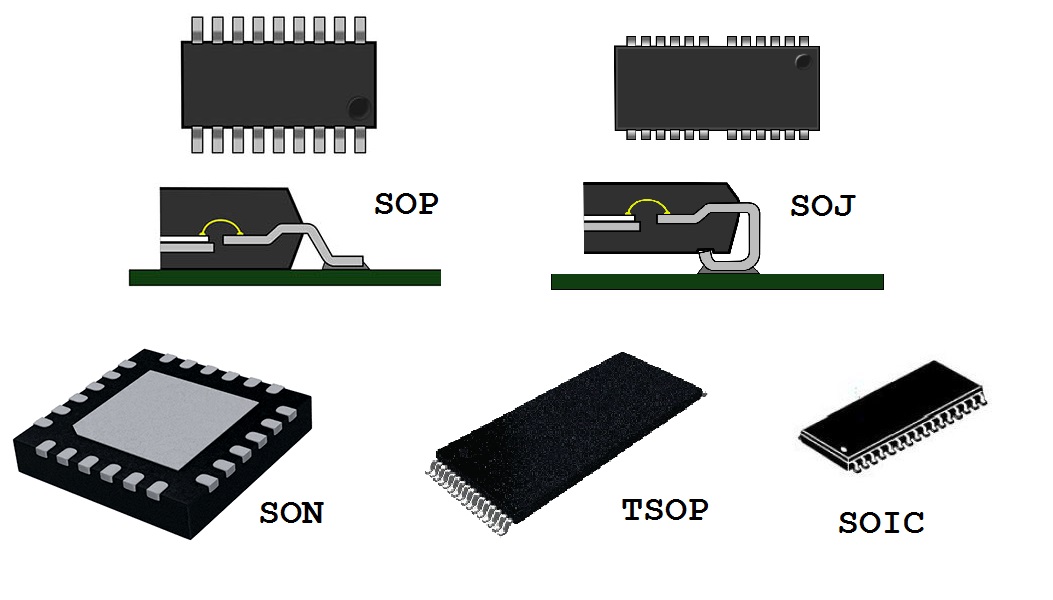
Surface mount
Despite the fact that there are a number of different methods that can be used to assemble electronic circuits, Surface Mount Technology (SMD) is still by far the most popular technique. This process allows for the production of modern devices with smaller footprints. This assembly method has many advantages and is highly customizable.
Unlike the earlier through-hole technology, SMT does not involve drilling holes in a circuit board. Instead, components are mounted directly to the PCB. This method allows for greater component density and is more cost-effective.
The manufacturing process starts with a pick-and-place machine that places components on solder paste. These components are then moved over a conveyor belt to a special reflow oven. This heating process is designed to melt the solder paste to a certain temperature and solidify it.
During this assembly process, the boards are checked for defects and if necessary, the excess solder paste is discarded. This method is the most cost-effective.